Lyles College of Engineering
Research
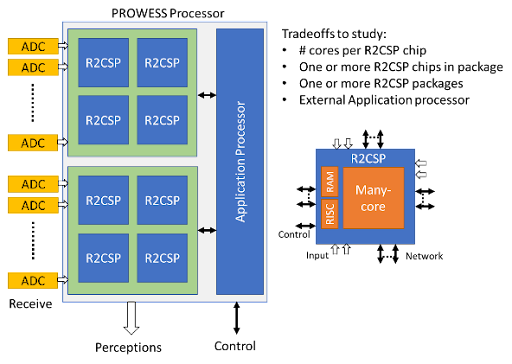
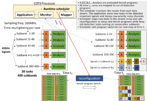
Runtime Reconfigurable Cognitive Spectral Processor (R2CSP)
Lead Researcher: Dr. Aaron Stillmaker
The project focuses on the development and fabrication of a fine-grained many-core
processing runtime reconfigurable spectral processor (R2CSP) for radio frequency (RF)
spectral sensing leveraging the KiloCore architecture and physical design developed
by Dr. Stillmaker. Dr. Stillmaker and his team at Fresno State are responsible for
the physical design of the R2CSP chip. The plan is to fabricate several test chips
in TSMC’s 16 nm technology. This multi-institutional project is led by Dr. David Zhang
from SRI in Princeton, NJ, with Dr. Bevan Baas as a Co-PI from UC Davis. The research
has received $13 million for the two and a half-year program scheduled to end in November
2025.
(a)
(b)
Figure 1. (a) PROWESS System architecture using R2CSP chips packaged as a multi-chiplet device
tested in Phase 2. (b) Example of 40GHz spectrum running high throughput on R2CSP
processing 200 MSample/s sub-bands with policy-based tasks designed to switch quickly
among different data streams and redeploy core resources to important signal processing
by reconfiguration.
Evaluation of Power Gate Implementation on Fine-Grained Many-Core Processor Arrays
Lead Researcher: Dr. Aaron Stillmaker
With larger, more complex digital designs, power gates become particularly necessary.
This project will explore the usage of power gates in large digital system to help
identify optimal usage. Power Gating is an effective method to reduce subthreshold
leakage and is straightforward to implement in large systems, but the implementation
becomes complex when implemented in a fine-grained methodology. The project will
explore design of power gates, placement of power gates, and algorithms for power
gate usage.
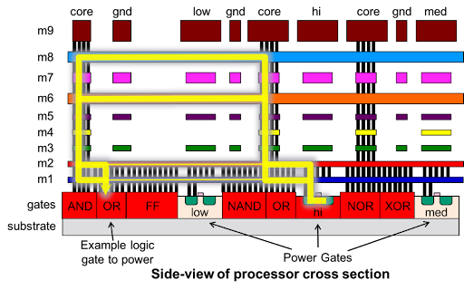
Figure 2. This is a diagram showing the flow of current from a power gate to an individual gate that needs to be powered. Power gates are usually PMOS devices that are controlled with “sleep” signals to turn the gates on and off based on some algorithm.
Area and Energy Efficient Full Duplex Transceiver System for Wireless Network on Chip
Lead Researcher: Dr. Soumyasanta Laha
Co-time co-frequency full-duplex wireless communication alleviates the issue of inefficient
use of bandwidth in the existing co-time half-duplex communication. In the full-duplex
mode the transmission and reception of the signal takes place simultaneously in the
same frequency band. The primary challenge in designing such a full-duplex wireless
device is self-interference. The transmit signal which is locally generated in the
transceiver and thus has a very high-power level interferes with the low power received
signal for being in the same frequency band. The received signal is thus submerged
in the ‘self-interfered noise’ and cannot be recovered. Several techniques have been
suggested over the last decade to reduce the self-interfered signal to the level where
it can be neglected, thus eliminating self-interference. The current project aims
to bring the self-interference cancellation to 60 dB or more, which is sufficient
for on-chip wireless communication such as wireless network on chips (WiNoCs). With
regards to WiNoC, this is important because, WiNoCs require high data rates (10 Gbps
and beyond) to support today’s high performance multi-core computer architecture and
require simultaneous data transfer to support real time applications. The expected
success of this research will motivate system level study with advanced sub-16 nm
RF FinFET technology at 60 GHz and sub-THz frequencies to evaluate and compare the
performance of existing and novel WiNoC architectures. Furthermore, the validation
of the full duplex transceiver system for WiNoC applications will expand research
insights for full duplex capability of other on-chip communications such as between
wireless enabled chiplets or a wireless neural accelerator architecture.
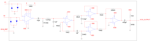
The current project is a novel co-time, co-frequency full duplex transceiver system
(See Fig. 1) for wireless network on chip (WiNoC) applications in a cost-effective
RF CMOS technology.
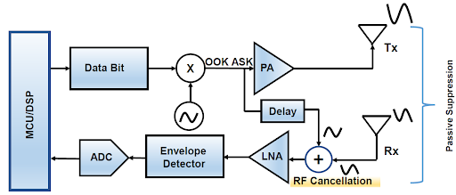 Fig. 1. Block Diagram of the proposed Full Duplex Wireless Transceiver.
Design and Testing Effectiveness of an AI based non-invasive glucose monitoring Device
Lead Researcher: Dr. Soumyasanta Laha
The worldwide prevalence of diabetes was 422 million in 2021. Hypoglycemia is a common
occurrence among insulin- dependent diabetics. Hypoglycemia unawareness results from
reduced sympathetic adrenal response and patients have difficulty recognizing hypoglycemia
events which puts them at high risk of adverse health events. These adverse health
events include cardiovascular ischemia, dementia, falls, and even deaths. Hypoglycemia-related
events resulted in 100,000 visits to emergency rooms and 30,000 hospital admissions
between 2007 and 2011 in the United States. On the other hand, poorly managed hyperglycemia
can also lead to adverse health events such as
cerebrovascular accidents, cardiovascular events, and peripheral vascular disease.
Prompt identification of rapid fluctuations in blood sugar is the key to successful
management of diabetes-related emergencies.
Continuous glucose monitoring (CGM) systems greatly improve self or parental management
by identifying particularly abnormal variations in the blood sugar and sending appropriate
alerts to patient’s phone or tablet have been helpful to identify fluctuations in
the blood glucose and can alert the patient thereby avoidance of severe outcomes related
to hypo or hyperglycemia. Current versions of CGM are minimally invasive where a metal
is inserted into the skin and serves as a sensor. It emits blood sugar oxidizing enzyme.
The interaction of this enzyme with blood sugar molecules results in the formation
of hydrogen peroxides amongst other compounds. The reaction also results in the generation
of a current. The charge on this current is measured and it corresponds to the appropriate
amount of blood sugar in the interstitial cells.
The project aims to explore the possibility of CGM using a non-invasive device at
the highest extent possible to enhance diabetic care integrating the two well established
detections methodologies: optical & electromagnetic. Specifically, a non-invasive
CGM prototype wireless system on chip (See Fig. 1) device as an application specific
integrated circuit (ASIC) integrating two detection methodologies will be implemented
using a robust AI/ML algorithm. 
Fig 1. The AI/ML based non-invasive glucose monitoring device as a wireless system on chip prototype.
The ML algorithms bring unprecedented accuracy and efficiency to the data analytic
results that have been traditionally relied on statistical and mathematical models.
In this study, the two detection methods of glucose monitoring are to be compared
against a commercial CGM device to train the ML model. The adaptive ML algorithm will
be particularly investigated to compensate for the absence of blood or other bodily
fluids in the non-invasive detection. The adaptive learning is a technique that is
applied in AI model development which provides a real-time instant result as a previous
data point is incorporated to reconfigure the model.
Prototype Shirt for Electrocardiography and Electromyography Analysis
Lead Researcher: Dr. Nan Wang
The use of textile-integrated sensors and systems has produced great interest in the
last years. Textiles are excellent interfaces for bio-signal sensing. They are flexible,
stretchable and conform to the body. As they are used daily and at all times, they
are an interesting solution for ubiquitous, continuous health monitoring. Breathing
rate and movement monitoring have been proposed and tested using extension sensors
based on knitted textiles made with textile conductive yarns, as well as using specially
made rubber coatings doped with carbon fibers, and conductive polymers. The sensing
techniques are evaluated for use in the development of a shirt integrating ECG/EMG
measurement, moisture detection and breathing movement detection for use in applications
such as monitoring of individuals in risk environments (firefighters, workers in specific
industries, etc.), sports, health monitoring for the elderly, continuous electronic
health records, or other.
Bulldog Mote- Low Power Sensor Node and Design Methodologies for Wireless Sensor Networks
Lead Researcher: Dr. Nan Wang
The major goals of the project are the design and implementation of the following
components: (1) efficient low-power methodologies implemented throughout all WSN design
layers from application to the physical layer, (2) a new WSN sensor node, the Bulldog
Mote, created using various low power methodologies, and (3) energy harvesting technologies
for sensor node architecture.
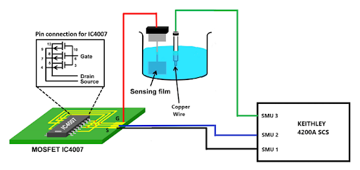
Extended-Gate Field Effect Transistor (EGFET)-Based sensor
Lead Researcher: Dr. Zoulikha Mouffak
This research is focused on the use of a EGFET sensor as a pH sensor or specific chemical
detector. We are exploring this setup to target biomedical applications. When the
MOSFET is connected to a sensitive electrode through the chemical solution we want
to analyze, the sensitive electrode works as an “extended gate”. Modification of the
solution concentration has resulted in changes in the drain current when running I-V
characteristics. We developed a ITO/PET EGFET pH sensor using ITO (Indium Tin Oxide)/PET
(Polyethylene Terephthalate) sensing electrode as the extended gate part of an EGFET
obtained from a combination of FETs from the CD4007 chip. The device was tested by
immersing the ITO/PET electrode in several chemical solutions of acidic and basic
nature, including hydrogen peroxide, acetic acid, sulfuric acid, and ammonium hydroxide,
at different concentrations. Using a Tektronix 4200A sourcemeter, we plotted the current–voltage
(I–V) characteristics for the different chemical solutions, and we established a correlation
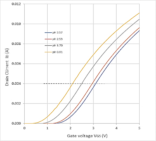
to the pH changes. Results from the plotted I–V characteristics show a great dependance
of the drain current (ID) on solution concentration (Fig. 3-b). The pH of the used
solutions established a relationship between the drain current and the pH value.
The results showed a consistent decrease in the current with an increase in the pH
value, although with different rates depending on the solution. The device showed
high voltage sensitivity at 0.23 V per pH unit when tested in sulfuric acid. These
results were recently published in Sensors. https://doi.org/10.3390/s23208350
 (a)
(a) 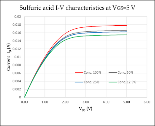 (b)
(b)
 (c)
(c) 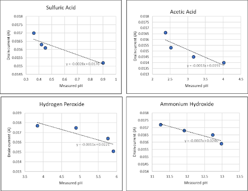 (d)
(d)
Fig. 1. Proposed EGFET schematic diagram (a), Sulfuric acid I–V characteristics for different
concent- rations for applied gate voltage VGS = 5 V (b), ID –VGS characteristics for
sulfuric acid aqueous solutions with concentrations of 10%, 1%, 0.1%, and 0.01% and
corresponding pH values 0.8, 1.70, 2.59, and 3.57 (c), and Drain current at VGS =
5 V and VDS = 4 V as a function of the measured pH of 4 solutions: sulfuric acid,
acetic acid, hydrogen peroxide, and ammonium hydroxide (d).

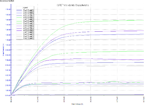
Fig. 2. EGFET I-V characterization using a porous silicon interdigitated capacitor as the
extended gate, measurement setup (left), and family of I-V characteristics obtained
from solutions of different concentrations (right).
Fabrication of Porous silicon (PSi) films for sensing devices
Lead Researcher: Dr. Zoulikha Mouffak
We investigate the fabrication of porous silicon using <100> silicon wafers with different
resistivities and varying anodization currents. Porous silicon is made using electrochemical
etching. During the etch process, the anode is connected to the metallized backside
of the silicon sample, while the cathode is connected to a platinum wire that we submerge
in an HF acid solution (Fig. 1). The applied constant current used and the resistivity
of the wafer define the pores size and quality, while the duration of the recipe defines
the thickness of the film. We analyze the surface morphology using scanning electron
microscopy (SEM) and photoluminescence tests (Figure 2). PSi films grown on higher
resistivity wafers show more luminescence and porosity.
(a) 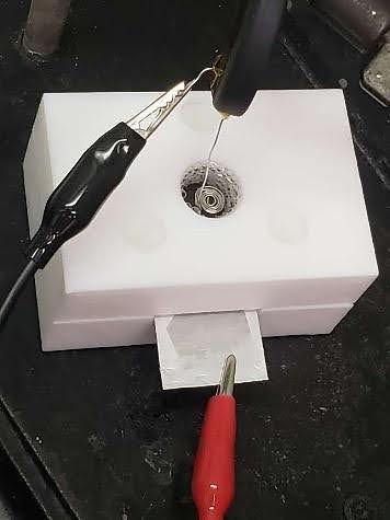 (b)
(b) 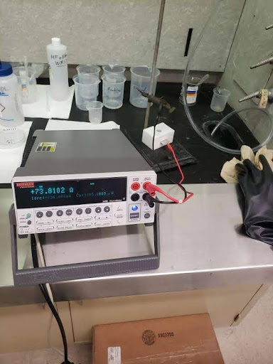 (c)
(c) 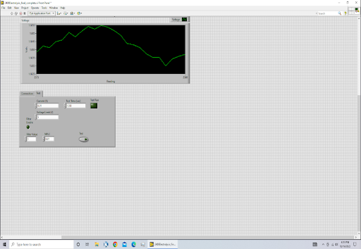
Fig. 1. Lab-made Electrochemical etch cell filled with HF and used for the fabrication of
porous silicon (a). The etch cell terminals are connected to a Keithley 2400 for constant
current supply (b. The recipe is run through Labview for a set time and restrictions
on voltage (c).
A digital twin-based condition monitoring method for power converters in agricultural
applications
Lead Researcher: Dr. Woonki Na
In this research. a digital twin-based condition monitoring method is proposed for
power converters in agricultural applications. The digital twin is a virtual replica
of the physical power converter and is able to update itself continuously as seen
in Fig. 1. The model is demonstrated or tested using various types of power converters,
including AC/DC, DC/DC, and DC/AC converters. The proposed digital twin system is
capable of updating itself continuously, which means it can reflect real-time changes
or conditions of the physical power converter, allowing for monitoring, analysis,
and potential optimization.
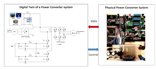
Fig. 1 Digital Twin Concept for Power Converters
Also, an artificial neural network (ANN) algorithm[1] is being used as part of the project.
The goal of applying the ANN algorithm is to minimize the difference between the output waveforms generated by the digital twin including fault diagnosis. These are the electrical waveforms produced by the power converter, which can include voltage and current waveforms. The digital twin is attempting to replicate these waveforms as accurately as possible. Thresholds are used as criteria to determine whether the digital twin's output is sufficiently close to the physical power converter's output. If the difference between the two waveforms falls within these thresholds, it's considered acceptable or successful. ANN would be used for optimization as well. It learns from the data generated by the digital twin and the physical converter to adjust its parameters and minimize the waveform differences.
Computer Arithmetic and Cryptographic Hardware
Lead Researcher: Dr. Hayssam El-Razouk
This research is focused on novel algorithms and hardware architectures for symmetric and asymmetric cryptosystems. Completed and current projects include efficient hardware for polynomial ring and finite field operations targeting post-quantum ciphers, Elliptic Curve Digital Signatures, Elliptic Curve Key Exchange, Advanced Encryption Standard (AES), Welch-Gong (WG) Stream Ciphers, and SNOW 3G/5G stream cipher. The research has also focused on developing designs for efficient hardware of fixed-point multipliers. Completed and current projects include low-area and low-power approximate fixed-point multipliers for machine learning and image processing applications.
Side-Channel Leaks
Lead Researcher: Dr. Hayssam El-Razouk
This research is focused on analyzing side-channel leaks in state-of-the-art cryptosystems like the Advanced Encryption Standard (AES), Elliptic Curve Key Exchange/ Digital Signatures, and Post-Quantum ciphers. Investigating novel countermeasures to improve the side-channel leak resistance of such cryptosystems. Completed and current projects include Differential Power Analysis (DPA) and countermeasures for AES, Elliptic Curve Key Exchange, and post-quantum ciphers.
Applied Cryptography
Lead Researcher: Dr. Hayssam El-Razouk
This research is focused on investigating novel applications for secure Internet
of things (IoT) and embedded systems. Completed and current projects include innovative
utilization of cryptography, Augmented reality (AR), and Bluetooth technologies for
building new applications targeting user accountability and privacy of digital data.
Innovative Nano-material Synthesis: toward the development, manufacturing, and characterization
of cutting-edge electro-active and photoactive nanomaterials and composites, ensuring
their suitability for advanced manufacturing processes
Lead Researcher: Dr. Sankha Banerjee
Research Project Description: This project is focused on the comprehensive creation,
production, and analysis of state-of-the-art electro-active and photoactive nanomaterials
and composites, ensuring their appropriateness for advanced manufacturing processes.
The objectives are (i) Fabrication/Synthesis Method Optimization: Develop and optimize
fabrication and synthesis methods, including simulation-based techniques, for thin
films and bulk active materials such as perovskite and MXene-based materials and composites.
(ii) Mechanism Investigation: Explore the mechanisms influencing material properties
by varying fabrication parameters and employing computational techniques. (iii) Microstructural
Analysis: Investigate the effects of physical relationships between different phases
in an electroactive material or composite and their impact on measured properties.
(iv) Characterization and Testing: Conduct thorough characterization and testing of
active nanomaterials utilizing electron microscopy and spectroscopic techniques. (v)
Optimization and Tailoring: Optimize and tailor material properties and performance
based on the parameters identified in the previous objectives and specific application
requirements.
Sub-project Example: Wet lab fabrication of Perovskite/Wurtzite-Oxide (e.g. ZnO, BaTiO3)
and 2D Materials-based (e.g. MXenes) flexible electro-active thin films with active
polymer and co-polymer matrices (e.g. PVDF/PVDF-TrFE)” - The purpose of this project
is to study the role of the dielectric and piezoelectric properties of graphene-based
composite piezoelectric materials. Due to its unique electrical and mechanical properties
such as it being stretchable up to 20% of its initial length and having high conductivity
due to the unidirectional structure with the ballistic transport of electrons, the
role of the 2D phase is critical in tailoring the electrical and mechanical properties
of the multiphasic composites.

Fig. 1: Scanning electron micrographs of the cross-section and synthesized thin film surface of active nanocomposite thin films, ZnO nanostructures such as nanowires, nano-flowers, and nanoflakes.
Smart Platforms for Health Monitoring of Devices and systems: The design and implementation
of intelligent systems utilizing advanced active nanomaterial systems to monitor and
assess the health of structures, particularly in advanced manufacturing processes
Lead Researcher: Dr. Sankha Banerjee
The objectives of this research area are centered around the development and implementation of agricultural health monitoring systems. The key goals include (i) Sensor Diversity for Agricultural Health Monitoring: Develop various types of sensors tailored for agricultural health monitoring systems, utilizing electro-active and photo-active perovskite/wurtzite and 2D structure-based materials. (ii) Optimization of Fabrication Techniques and Design Parameters: Modify fabrication techniques and design parameters of the materials to enhance their dynamic properties. (iii) Energy-Efficient Wireless Sensor Networks for Agriculture: Design energy-efficient wireless sensor networks specifically for agricultural health monitoring systems. (iv) Real-time Analysis and Machine Learning for sensor application feasibility: Perform real-time analysis of streaming data and develop machine learning models to forecast the health and progressive damage of agricultural structures under various conditions, including aging and extreme loads.
Sub-project Example: “Study of the Efficacy and economic feasibility of a perovskite-oxide
based active-sensor Non-Invasive Glucose Monitoring System Using Infrared Light Intensity
Correlations: Toward the Development of Measurement Metrics Using Data Analytics for
monitoring plant health” The goals and objectives of this subproject are to verify
the feasibility of non-invasive optical glucose monitoring using light intensity correlations
based detection mechanism continuously in by adapting wearable form-factor using Flextronics
and advanced signal processing techniques to assess and monitor plant health. Data
collected at each glucose concentration are compared to establish a correlation between
the glucose concentration and the refracted light voltage reading. After evaluating
performance characteristics, via Mean Absolute Error (MAE), Mean Squared Error (MSE),
and Coefficient of Determination (R2), a Decision Tree Regression model displayed
the greatest overall performance values.

Figure 2. Non-invasive nutrient monitoring system including comprehensive machine learning
process flow in Dr. Banerjee’s laboratory [6, 7, 8].
Heterohenous Integration
Lead Researcher: Dr. Nusrat Jahan
Full-duplex wireless systems use breakthrough technology enabling simultaneous transmission and reception on the same frequency, boosting spectral efficiency. Circulators, particularly Gallium Nitride (GaN)-based, enhance signal processing. III-V semiconductor technologies like GaN, Gallium Arsenide (GaAs), and Indium Phosphide (InP) are distinguished by their high breakdown voltages and thermal stability due to their material properties. GaN, in particular, boasts a significantly higher bandgap energy level (3.4eV) compared to Silicon (1.1eV), resulting in devices with faster, lower-loss switching operations.
Integrating CMOS for clock generation alongside GaN in active circulator design tackles
complexity, enhancing performance in Full-Duplex (FD) radio systems.
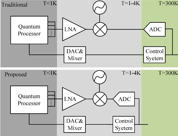
Cryogenic Electronics Design
Lead Researcher: Dr. Nusrat Jahan
Designing control and readout blocks for qubits in quantum computing, implemented
in CMOS technology. Qubits operate differently from classical bits, existing in superpositions
of 0 and 1 states. Quantum processors, with qubits functioning at ultra-low temperatures,
require architectures that perform well under cryogenic conditions to unleash quantum
computing's full potential and push computational boundaries.